Monday 20 January 2014

Home Monitoring System – Sensor Node

Finally the boards that I designed for the home monitoring system arrived from OSH Park. Son now I can get down to building the the boards. The photo below shows the board in the bottom half of the enclosure that I am planning to use.
WP_20140116_003
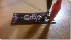
To ensure that I don't release the blue smoke I decided to build and test the node in a number of steps. For the first step I soldered the components of the power supply and tested the output voltage.
WP_20140116_004
This first step was successful connecting a bench power supply set to 2.8 volts yielded an output of 3.3 volts.
WP_20140116_005
The next step was to solder the remaining capacitors and ICs and resistors. When designing the board I used 0603 for the resistor and capacitor footprints. This was a mistake because they are difficult to hand solder due to the size. Next time I will use the next size up.

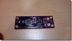
The other SMD that was difficult to solder was the LCC8 humidity sensor. In fact I initially soldered it on upside down and had to remove it, in the process of which I destroyed the part. Below is an image of the final board with the debug and ISP header but without the radio module this will be added later.
WP_20140117_004
When I initially attached the ISP I found that it would not connect to the board. The reason for this was that the ISP clock was set to the default of 1Mhz. The ATmega48PA is shipped with internal RC oscillator at 8.0MHz and with the fuse CKDIV8 programmed, resulting in 1.0MHz system clock. Reducing the ISP clock to 1/4 of the CPU frequency resolved the issue.
AVRSettings
When I resolved the connection issue to the device I was able to flash the firmware and start testing the sensor board. The first check was to determine if the ADC voltage monitoring circuit worked. This is where I ran into another problem. I powered the board with a bench power supply @ 2.8 volts. Reading the battery voltage via the ADC resulted in a value of 2.1 volts. After examining the battery sensing circuit it initially looked like the p channel FET was not switching on fully causing a voltage drop of 0.6 volts across the Source to Gate. Checking the Drain voltage measured 2.1 volts which was wrong because it was not switched on, i.e. 0 volts applied.

On a hunch I checked the datasheet of the FET against the footprint on the board. I discovered the PMBFJ177 footprint is different the Gate and Drain are interchanged. I will need to get another J177 FET that matches the board footprint.

Once these issues where resolved I was able to debug the code that reads the humidity and temperature from the CC2D33S sensor using the AVR dragon.

The next step is to add the radio module and figure out a strategy to debug and test the radio module and its code.
Saturday 4 January 2014

Home Monitoring System – Phase 1

Having spent a great deal of time and effort upgrading my 1970s built home to make it habitable in the winter, yes it was really that bad, and as an added benefit improve its energy efficiency. Now that the improvements have been made I would now like to monitor the effectiveness or lack thereof if that happens to be the case. Unfortunately I have will have no data to compare the data acquired from this proposed system, on the up side I will have data to hopefully make further improvements.

My initial plan is to focus on space heating as this is generally the biggest pain point in older houses.

Goals

  • Capture Temperature and Humidity
    • Temperature and Humidity are related and have an effect on the Thermal Comfort of the living space
  • Small Size Sensors
    • The sensors must be small and inconspicuous as I will be placing a number of them around the house
  • Battery powered
    • AA or AAA batteries, preferably AAA due to the size requirement
  • Efficient Power Usage
    • Aim to be operational for minimum of a year without requiring a battery change

Solution

Sensor

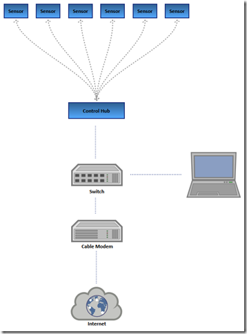
For phase 1 the wireless sensors will communicate with the Control Hub which will log and aggregate the data that the sensor nodes periodically send. The control hub will expose a set of web pages to manage the sensor network devices and view and export data.

Sensor Node

The sensor node is based around an Atmel ATMEGA48PA 8-bit CPU. This was chosen due to the fact that it is a picoPower device which means that it is capable minimising power down to 0.1µA in sleep mode.

The wireless link will use an nRF24L01+ module these are extremely cheap and can be picked up on eBay for 80 cent which is remarkable given the chip itself is about 2-3 euro in single unit prices. This device operates in the 2.4Ghz space and is optimised for low power applications. Consuming sub μA current in power down mode.

To measure humidity and temperature the sensor chosen was the CC2D33S sensor from GE. This sensor has a 3% accuracy and operates from –40 to 125°C. It costs about 6 ~ 8 euro in single unit quantity. It has an I2C bus interface and can operate in a sleep mode where it consumes 0.6 µA (typical) and 750 µA (typical) when operating. It also has a small footprint compared to some of the cheaper Chinese sensors available.

For power management I decided to add a boost regulator based on the 3.3 volt version of the AAT1217 chip. This was chosen due to cost and the fact that it does not need an external Schottky diode which are difficult to find with a low forward voltage drop and reasonable load current.

PowerSupply

The boost regulator will operate down to 0.5 volts ensuring that the sensor node will remain operational as the input voltage drops.

I have also added the option of not installing the boost convertor and its components by placing a shut from VBAT to VCC.

Shunt

To monitor the input voltage to the sensor node I added a simple FET switch switch to a resistor that that the microcontroller will sample when it is performing a sensor update and send the input voltage, temperature and the humidity data.

BatSense

I will use the following enclosure to house the sensor as its neat and tidy. The PCB to fit the chosen enclosure was designed with KiCad and a small batch was ordered through OSH Park. A render of the PCB is shown below.

i

Once the boards arrive I will begin the building and debugging. I will add some follow up posts recording my progress. I think the main risk to the sensor nodes is the radio module. The 2.4 Ghz band is quite congested and the range performance of the 2.4 Ghz modules can be affected by obstacles such as internal doors, floors and walls.

Control Hub

The Control Hub is the next piece of the system, I have not made much progress on the implementation of this yet. I do however have a set of requirements:

  • Expose a simple web interface
    • To view data
    • To manage the sensor nodes, update interval etc.
  • On board storage
    • Should not require external storage for storing reading
  • Expose  a programmatic interface
    • Maybe some kind of restful interface